General, quoting & support.
Add: Building E, No.58, Nanchang Road, Xixiang , Baoan District Shenzhen City, Guangdong, China
Tel : 0755-27348887
Fax : 0755-27349876
E-mail : svc@pcbastore.com
What is HDI PCB? Why?
aaron / 2017-07-21
Contents [hide]
What Is HDI PCB?
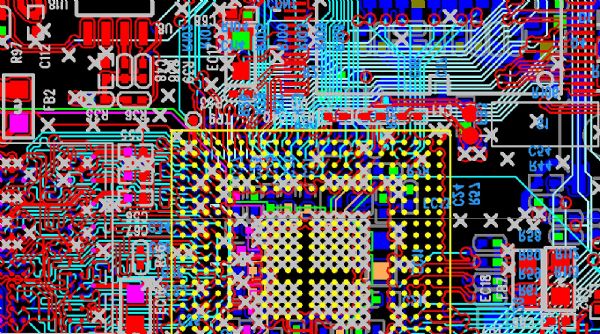
HDI PCB is a circuit board which has a larger wiring density per unit area compared to a conventional board. The HDI in HDI PCB means High Density Interconnector.
It has a higher quantity of interconnections and at the same time, occupy a smaller space. Components are placed closer to each other but functionality is still of top quality. A PCB with 120 to 160 pins per square inch is already an HDI PCB. The circuitry is executed with the use of microvias, buried vias and blind vias and imbedded through laser drilling.
Computers that you use are no longer bulky. They have become more fashionable, sleek and chic. HDI PCBs have enabled them to be smaller, just like human models on the fashion ramp who need to be thin so that they can fit into the clothes that they market. These devices no longer have the utilitarian look which leaves nothing to the imagination.
You can also watch Netflix movies on your super thin smartphones, which at times, have even more powerful circuit boards than your PCs and laptops. Or also plug in your wireless headphone which also has its own well designed HDI PCB and enjoy the lifelike acoustics.
All these are possible because of miniaturization of many things electronic and electric, without compromising the quality and signal relay.

Different Types of HDI PCB
Through vias from surface to surface
With buried vias and through vias
Two or more HDI layer through vias
Passive substrate without electrical connection
Coreless construction utilizing layer pairs
Alternate production of coreless constructions with the use of layer pairs.
Benefits of HDI PCB
1) Phenomenal Versatility
HDI PCBs are used a wide array of functions. Their capability to be smaller, functional and more portable makes them suitable for use in wearable technology, automotive, military, aerospace, communications and healthcare.
2) Compact Design
The creative mixing of buried vias, blind vias and microvias on the circuit board helps bring down considerable the space and weight allotment.
3) Better Signal Integrity
The components are set closer to each other to make the signal path length shorter. This is made possible through via in pad and blind via technology.
4) High Reliability
These stacked vias on the boards are extremely reliable in extreme environment temperatures and annoyances.
5) Faster Time to Market
The vias and components are easier and faster to install on the boards. This makes it possible for a shorter time from design and testing to fabrication, and then finally to marketing.
6) Cost Effective
The quality is not compromised when a standard 8 layer through hole board (standard PCB) is made smaller into a 6 layer HDI board. Thus, when bulk quantity of HDI PCBs are manufactured, it will be cost effective.
Design Tips for HDI PCB
For the stackup, don't use more than 3 sequential layers unless absolutely necessary.
Use a good fan out design for difficult ICs like QFNs and BGAs so you can minimize the count of your sequential lamination if you plan your fan out properly.
The layout of the components of the board should always consider the criteria of installability, solderability and maintainability.
PIN spacing. Between PIN and SOP it should be at least 40 mil; between PIN and BGA, at least 80 mil.
Include a definite isolation effect for the bottom and top layer components so you can decrease inner layer signal crosstalk.
The wise use of vias - microvias, buried or blind - is a sensitive decision that lays out the direction of the manufacturing process, the choice of equipment and the processing time.
The selection of components is critical for determination of trace widths, locations and also the sizes and types of drill holes and stackup. Performance superiority, packaging, traceability and availability should also be of prime consideration.
Route traces in such a way that signal integrity issues are not compromised.
Use a PCB stackup that reduces manufacturing costs. The material types and the number of layers directly impact the quantity of lamination and drilling cycles required
Different HDI PCB Stackups
1) HDI PCB (1+N+1)
The simplest HDI. It is best for BGA with lower I/O counts. Its fine line, microvia and registration technologies are capable of 0.4 mm ball pitch. It undergoes qualified material and surface treatment for a lead free process. It also has excellent mounting stability and reliability and has copper filled via.
Its applications are for cell phone, UMPC, MP3 player, PMP, GPS and memory card.
2) HDI PCB (2+N+2)
It is a moderate complex HDI. Designed for BGA with smaller ball pitch and higher I/O counts. It has thin board capabilities and can increase routing density in complicated design. It has copper filled via and the lower Dk/Df material enables improved signal transmission quality.
Its applications are for cell phone, UMPC, PDA, DSC, portable game console and camcorder.
3) ELIC (Every Layer Interconnection)
It is the most complex HDI. The every layer via structure maximizes freedom of design. Its copper filled via provides better reliability and superior electrical features. It uses Cu bump and metal paste technologies for its very thin board.
Its application is for cell phone, PMP, GPS, UMPC, MP3 and memory card.
The Differences Between HDI PCBs and Standard PCBs
Standard PCBs:
Lesser component density per square inch
Larger and bulkier boards
Through holes mechanical drilling
Higher number of layers
May encounter compatibility issues with low pitch packages
HDI PCBs:
Higher component density per square inch
Smaller and lighter boards with better functionality
Laser direct drilling of buried, blind and microvias
Lower number of layers
Highly compatible with high pin count and low pitch packages
The HDI PCB Manufacturing Process
It is the procedure which transforms a circuit board design into an actual physical structure based upon agreed specifications in the design package. Here are the HDI PCB manufacturing steps:
Imagine the desired layout on copper clad laminates
Etching or the removal of excess copper from inner layers to reveal traces and pads
Execute the PCB layer stackup through laminating (through heating and pressing) board materials at high temperatures
Drilling holes to mount holes, through hole pins and vias
Etching or the process of removing excess copper from the surface layers to reveal traces and pads
Plate the pin holes and via holes
Put protective coating to surface or solder masking
Silkscreen printing reference and polarity indicators, logos and other markings on the surface
As an option, add a finish to copper areas of the surface.
Application Scenarios of HDI PCB
1) Healthcare
They are used in scanning equipment (x-ray screens, CT scanners, ultrasonic scans), medical monitors (blood glucose, heart rate, blood pressure), medical instruments (electronic microscopes, control systems, compressors).
PCBs are used in colonoscopy equipment. They enable miniature camera size wherein the inner parts of the patient can be observed and the correct diagnosis can be relayed to the patient. Yes, the cameras are smaller but the picture quality is excellent. Before, people find it discomforting to be inserted with a tube, but these smaller equipment, thanks to PCBs, a colonoscopy procedure won't hurt anymore.
2) Automotive
Satellite navigation, advanced dashboards (connect to car*s radio or media player), control systems (power supplies, fuel regulators, engine management), proximity monitors (built in sensors to monitor blind spots and measure distances, accident prevention).
Car makers are attracted by the potential of small sized PCBs because they save space inside the automobile. Futuristic vehicles from Tesla integrates electronic devices to improve driving experience for motorists and also to protect them from accidents.
3) Smartphones, Tablets and Computers
PCBs are foundations for smartphones, smart watches, tablets and radios. Computers like home desktop PCs, workstations, laptops and satellite navigation have PCBs at their core.
4) Wearable Technology
The Apple Watch, IoT and other wearable devices like virtual reality headsets. This market segment is gaining ground in the youth segment.
5) Military and Aerospace
Military communications devices and other strategic defense equipment like missile systems. HDI PCBs are designed for extremely dangerous environment conditions.
HDI PCBs Will Be Here to Stay
HDI PCBs have important roles in everyday modern life as technology increasingly shows its presence in our daily routines. These advanced circuit boards even have become platforms or foundations because they are existent in almost any device or appliance that is sourced electrically or electronically.
Being a constant reality in our lives, PCBs come in various configurations which serves different functions which makes our daily grind easier and more relaxed. And also allows us more time for recreation, which astonishingly, also involves PCBs to a heavy degree.
As technology advances, and the world grows and adapts, HDI PCBs will continue to play a vital role in all the important things that we use.
Life spans will be increased, leisure time will be more hours per day (compared to work hours), and motoring accidents will be nearly zero statistically because of these amazing advanced circuit boards which have a life of their own.

We're capable of manufacturing HDI PCB up to 40 layers in various structures. For HDI PCB production price, please send your PCB file (Gerber format of file preferred) & requirements to svc@pcbastore.com, we'll quote ASAP.
Previous article:PCB Introduction and Categories


